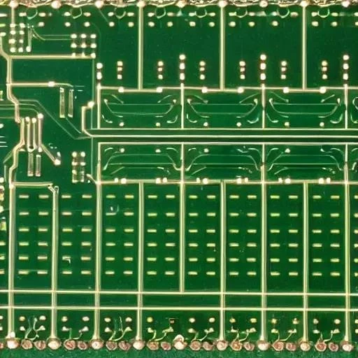
In an age increasingly defined by digital innovation, where every device, from the smartphone in your pocket to the autonomous vehicles navigating our roads, hums with intricate intelligence, there exists a foundational technology that often remains unseen, yet is profoundly indispensable: the printed circuit board (PCB). These remarkably intricate layers of conductive pathways and components are not merely green boards; they are the veritable nervous system of modern electronics, orchestrating complex operations with astonishing precision. Without them, the sophisticated world we inhabit would simply cease to function, reverting to an era of bulky, unreliable point-to-point wiring.
The journey of creating a PCB is a captivating blend of meticulous engineering, cutting-edge material science, and artistic design, transforming abstract ideas into tangible, functional realities. It’s a process that has evolved dramatically from its rudimentary beginnings, now driven by advanced software, automated manufacturing, and an insatiable demand for smaller, faster, and more powerful devices. This ultimate guide will meticulously demystify the fascinating world of PCB creation, offering a forward-looking perspective on how these vital components are shaping our technological future and empowering innovators worldwide to push the boundaries of what’s possible.
| Aspect of PCB Creation | Description | Importance/Impact | Key Tools/Resources |
|---|---|---|---|
| Schematic Design | Conceptualizing the electronic circuit, defining components and their interconnections. | Establishes the functional blueprint; critical for circuit integrity and performance; | Altium Designer, KiCad, Eagle, OrCAD |
| PCB Layout | Translating the schematic into a physical board design, including component placement and trace routing. | Determines the board’s physical dimensions, signal integrity, and manufacturability. | Altium Designer, KiCad, Eagle, SolidWorks PCB |
| Fabrication File Generation | Creating industry-standard files (Gerber, Drill files) for manufacturing. | The universally accepted language for PCB manufacturers to produce the physical board. | Built-in features within design software (e.g., Altium, KiCad) |
| Manufacturing Process | Physical production of the bare board, involving etching, drilling, plating, and layering. | Transforms the digital design into a tangible, multi-layered substrate ready for components. | PCB fabricators, specialized machinery (e.g., CNC drills, etchers) |
| Assembly (SMT/Through-hole) | Populating the bare board with electronic components using soldering techniques. | Brings the circuit to life, connecting all components to form a functional device. | Pick-and-place machines, reflow ovens, soldering irons, component suppliers |
| Testing & Quality Control | Verifying the functionality, integrity, and performance of the assembled PCB. | Ensures reliability, prevents failures, and meets design specifications. | In-Circuit Testers (ICT), Flying Probe Testers, Oscilloscopes, Visual Inspection |
From Concept to Reality: The Design Imperative
The journey commences with the design phase, where innovative ideas take their first concrete form. Engineers meticulously translate complex circuit diagrams into a digital blueprint using sophisticated Electronic Design Automation (EDA) software like Altium Designer, KiCad, or Eagle. This initial step, known as schematic capture, is akin to an architect sketching the foundational plans for a grand edifice, precisely detailing every component and its logical connections. By integrating insights from AI-driven tools, designers can now optimize component selection and placement, significantly reducing development cycles and preempting potential issues with remarkable efficiency.
Following schematic capture, the layout phase begins, a critically important stage where the abstract circuit is transformed into a physical representation on the board. Here, components are strategically placed, and conductive traces – the “highways” for electrical signals – are meticulously routed across multiple layers. This demands an acute understanding of signal integrity, thermal management, and manufacturability. Through rigorous simulation and design rule checks (DRC), potential conflicts and performance bottlenecks are identified and resolved, ensuring a robust and reliable design; Expert opinions consistently highlight that a well-executed layout can drastically improve product performance and reduce manufacturing costs, underscoring its pivotal role.
The Art of Fabrication: Bringing Blueprints to Life
Once the digital design is perfected, it’s exported into industry-standard Gerber files and drill files, which serve as the definitive instructions for fabrication. These files are then sent to specialized PCB manufacturers, initiating the physical transformation. The fabrication process is a marvel of modern engineering, involving a series of intricate steps: layering substrates (most commonly FR-4, a glass-reinforced epoxy laminate), photo-imaging the copper traces, chemical etching to remove unwanted copper, precision drilling of holes for component leads and vias, and electroplating to enhance conductivity and structural integrity. Each step is meticulously controlled, with advanced automation ensuring unparalleled accuracy and consistency across production batches.
The sheer complexity of modern multi-layer PCBs, often featuring dozens of layers, is a testament to human ingenuity. Imagine a microscopic, three-dimensional city, with countless highways and tunnels facilitating the flow of information – that’s essentially what’s being created. This intricate layering allows for incredibly dense component packing and optimized signal paths, profoundly impacting the performance of everything from high-speed servers to compact medical implants. Industry examples abound, from the compact logic boards powering Apple’s iPhones to the resilient PCBs found in spacecraft, each a testament to the versatility and reliability of this manufacturing marvel.
Assembly and Beyond: The Future of Interconnectedness
With the bare board fabricated, the next critical phase is assembly, where electronic components are precisely mounted and soldered onto the PCB. This involves both Surface Mount Technology (SMT), where tiny components are soldered directly onto the board’s surface, and through-hole technology for larger, more robust components. Automated pick-and-place machines, operating with astonishing speed and accuracy, are at the forefront of modern assembly lines, capable of placing thousands of components per hour. Following component placement, reflow soldering creates robust electrical and mechanical connections, bringing the circuit to life.
The final, yet equally crucial, stages involve rigorous testing and quality control. From in-circuit testing (ICT) to functional testing, every assembled board undergoes a battery of checks to ensure it meets exacting performance specifications and reliability standards. Looking forward, the PCB industry is experiencing rapid innovation. Flexible PCBs are revolutionizing wearable technology and medical devices, allowing electronics to conform to non-planar surfaces. The integration of advanced materials, such as those enabling higher frequency operation or enhanced thermal dissipation, is pushing the boundaries of what’s achievable. Furthermore, the advent of AI in design optimization, predictive maintenance for manufacturing equipment, and even self-repairing circuits promises a future where PCBs are not just integral, but increasingly intelligent and adaptive.
The printed circuit board, far from being a static component, is a dynamic frontier of innovation, continuously evolving to meet the escalating demands of our interconnected world. As we continue to miniaturize devices, accelerate data transfer, and explore new frontiers in areas like quantum computing and advanced robotics, the foundational role of the PCB will only grow in importance. Mastering its creation is not just about building circuits; it’s about empowering the next generation of technological breakthroughs, shaping a future where possibilities are limited only by our collective imagination. The future, undoubtedly, is built on these tiny, yet incredibly powerful, green boards.