In today’s technologically advanced world, it’s easy to take for granted the intricate systems that enable our devices to function. At the heart of nearly every electronic gadget, from smartphones to sophisticated medical equipment, lies a silent workhorse: the Printed Circuit Board (PCB). These unassuming green (or sometimes other colors!) boards are the unsung heroes of the digital age, providing the essential pathways for electrical signals to flow, allowing our devices to compute, communicate, and connect us to the world. But how exactly does a PCB work, and why is it so crucial to modern technology?
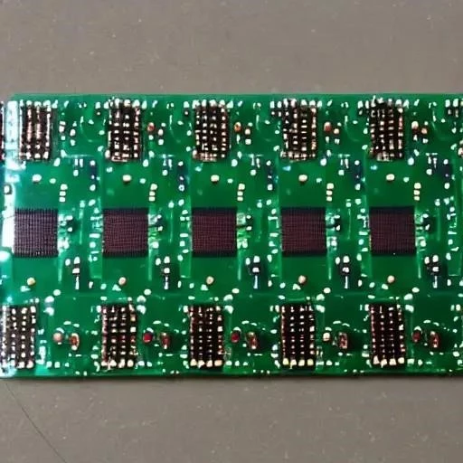
A Printed Circuit Board is more than just a flat piece of material; it’s a meticulously designed network of conductive pathways, typically made of copper, etched onto an insulating substrate. These pathways, known as traces, act like tiny highways, guiding electrical signals between various electronic components such as resistors, capacitors, integrated circuits, and connectors. By precisely connecting these components, the PCB allows them to work together harmoniously, performing specific functions within a device. Imagine a city’s road network, carefully planned to ensure efficient traffic flow; a PCB operates on the same principle, but with electrons instead of cars. The evolution from laborious point-to-point wiring to PCBs drastically improved reliability and reduced failures, paving the way for the miniaturization and mass production of electronics we see today. Learning the basics is the first step, and with readily available resources like Arduino starter kits and design software such as KiCAD, getting started is easier than ever.
Key Components and Functionality of PCBs
Understanding the anatomy of a PCB helps to appreciate its intricate functionality. Let’s delve into the essential elements that make up a typical printed circuit board:
- Substrate: This is the base material of the PCB, usually made of fiberglass-reinforced epoxy laminate (FR-4) for its strength and insulation properties.
- Copper Layers: Thin layers of copper are laminated onto the substrate and then etched to create the conductive traces that carry electrical signals.
- Solder Mask: A protective coating applied over the copper traces to prevent oxidation, reduce the risk of short circuits, and ensure solder only adheres to designated pads during component assembly.
- Silkscreen: A layer of epoxy ink used to print component labels, logos, and other identifying marks on the PCB.
- Vias: Small holes drilled through the PCB to connect traces on different layers, enabling complex circuit designs.
The Manufacturing Process: From Design to Reality
The journey of a PCB from design to a finished product is a fascinating blend of art and science, involving several precise manufacturing steps. Here’s a simplified overview:
- Design: Using Electronic Design Automation (EDA) software, engineers translate a circuit schematic into a detailed PCB layout.
- Printing: A photo-sensitive film is exposed to UV light through a mask, transferring the circuit pattern onto the copper layer.
- Etching: Unprotected copper is chemically etched away, leaving the desired traces.
- Drilling: Holes are drilled for vias and component mounting.
- Plating: Vias are plated with copper to create electrical connections between layers.
- Solder Mask Application: The solder mask is applied and cured to protect the copper traces.
- Silkscreen Printing: Component labels and other markings are printed on the PCB.
- Testing: The finished PCB is tested to ensure it meets design specifications.
The Future of PCBs: Innovation and Advancements
As technology continues to evolve at an unprecedented pace, PCBs are adapting to meet the demands of increasingly complex and miniaturized devices. Innovations such as high-density interconnect (HDI) PCBs, flexible PCBs, and embedded components are pushing the boundaries of what’s possible. These advancements are enabling the creation of smaller, more powerful, and more reliable electronic devices, driving innovation across various industries. Imagine flexible circuits seamlessly integrated into wearable technology or high-performance PCBs enabling faster and more efficient data processing in next-generation computers. The future of PCBs is bright, promising even more exciting developments that will shape the world of electronics for years to come.